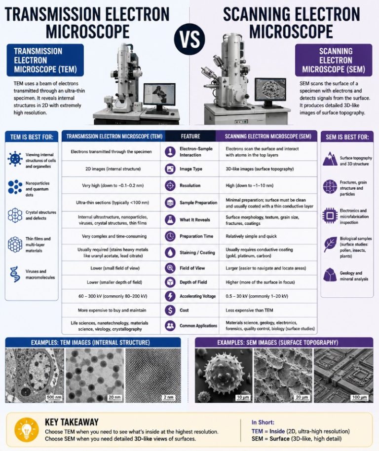
Transmission electron microscopes and scanning electron microscopes both fire beams of electrons at a specimen — but one fires through it and the other scans across it, and that single difference determines almost everything else: what you can see, how you prepare the sample, and which instrument you reach for first.
TEM vs SEM: quick comparison
| Feature | TEM | SEM |
|---|---|---|
| Imaging principle | Electrons transmitted through the specimen | Focused beam rastered across the surface |
| Accelerating voltage | 60–300 kV | ~1–30 kV |
| Best resolution | Sub-50 pm (aberration-corrected); ~1–2 Å typical | ~1 nm (FE-SEM at 30 kV); 3–25 nm (tungsten source) |
| Magnification | Up to ~50 million× | ~10× to ~1–2 million× |
| What you see | Internal structure / atomic columns (2D projection) | Surface morphology & topography (3D-looking) |
| Depth of field | Low | Very high — entire rough surface stays sharp |
| Sample thickness | <100 nm (ultrathin section required) | Bulk (mm-scale) acceptable |
| Sample prep | Fixation → embedding → ultramicrotome or FIB → staining | Conductive coating (e.g. sputtered Au) for non-conductors; otherwise minimal |
| Image dimensionality | 2D projection (3D via tomography/STEM) | 3D-looking surface topography |
| Typical applications | Crystal lattice, atomic bonding, viral capsid structure, protein complexes | Surface morphology, fracture analysis, semiconductor inspection, elemental mapping (EDS) |
How a transmission electron microscope works

A TEM generates a high-energy electron beam — accelerated by voltages of 60–300 kV — from an electron gun fitted with a tungsten filament or, in modern instruments, a field-emission source. That beam passes through a series of electromagnetic condenser lenses that shape and focus it, then transmits straight through an ultrathin specimen section.
As electrons travel through the sample, they scatter. Dense or heavy-atom regions (like osmium-stained cell membranes or metal atoms in a crystal) scatter strongly and appear dark; open regions with few atoms transmit electrons and appear bright. The objective lens captures the transmitted electrons and magnifies the resulting diffraction pattern and phase-contrast image, which is then projected onto a fluorescent screen, photographic plate, or — in modern instruments — a direct electron detector or CCD camera with fiber-optic coupling.
The critical practical constraint: the specimen must be thinner than roughly 100 nm so electrons can actually make it through without being completely absorbed or scattered beyond recovery. For biological samples, this means chemical fixation in glutaraldehyde and osmium, resin embedding, and ultramicrotome sectioning with a diamond knife. For hard materials — ceramics, semiconductors, alloys — a focused ion beam (FIB) mills a site-specific lamella to electron transparency. Either way, TEM sample preparation is the most demanding in electron microscopy. A good prep tech is worth their weight in gold.
The payoff: TEM resolves individual atoms. Aberration-corrected instruments (Cs correctors, introduced commercially in the early 2000s) push resolution below 50 pm — sub-Ångström — which is smaller than the diameter of a hydrogen atom. You can see crystal lattice fringes, atomic columns, and point defects. No other bench instrument comes close.
How a scanning electron microscope works


A scanning electron microscope works on a completely different principle. Rather than transmitting electrons through the specimen, it focuses a narrow beam — accelerated at 1–30 kV (much lower than TEM) — and rastering it across the specimen surface in a rectangular pattern. The beam never passes through; it interacts with only the top few nanometers to a few micrometers of material, depending on accelerating voltage.
That interaction generates several distinct signals, each telling you something different:
- Secondary electrons (SE): low-energy electrons (<50 eV) ejected from the near-surface (~5–10 nm). They’re highly localized to where the beam hits, which is why SE images have the crisp, high-resolution surface topography SEM is famous for. An SEM image of a fracture surface or a mosquito’s compound eye uses SE signal.
- Backscattered electrons (BSE): high-energy electrons elastically reflected from deeper in the specimen. BSE yield is proportional to atomic number (Z) — heavier elements backscatter more electrons and appear brighter. A BSE map of a polished alloy section shows you compositional contrast at a glance, with each phase a different shade of grey.
- Characteristic X-rays (EDS/EDX): when the beam ejects an inner-shell electron, an outer-shell electron drops in to fill the vacancy and releases an X-ray with energy characteristic of that element. An energy-dispersive X-ray spectrometer (EDS or EDX) attached to the SEM collects these X-rays. The result: point analysis, line scans, or full elemental maps that identify what every spot on the surface is made of. EDS is SEM’s killer application in materials science — you can identify phases, check coating composition, or trace contamination across a semiconductor wafer in a single session (Bruker: What is EDS?).
Because SEM scans the surface and can handle bulk, mm-thick samples, sample preparation is minimal compared to TEM. The main requirement: the specimen must be electrically conductive so charge doesn’t build up under the beam and produce distorted, artifact-ridden images. Metals, semiconductors, and carbon-coated specimens are fine as-is. Non-conducting materials — ceramics, polymers, biological tissue — need a thin conductive coating, usually a few nm of sputtered gold or gold-palladium. The first time you forget this and watch a charging artifact wash out your image in real time, you never forget again.

SEM’s other major practical advantage over TEM: its enormous depth of field. Where a compound light microscope renders only a thin focal plane sharp at any given focus setting, an SEM keeps a rough fracture surface, a pollen grain, or a circuit board edge sharp from front to back simultaneously. That’s why SEM images have the dramatic, almost three-dimensional quality that light microscopy can’t match.
Magnification
TEM magnifies up to approximately 10–50 million times — the highest of any electron microscope. SEM covers a much wider practical range, from as low as 10× (comparable to a hand lens) up to roughly 1–2 million× on top field-emission instruments, making it uniquely versatile for both low-mag survey work and high-mag surface detail in the same session.
A note on empty magnification: magnifying beyond what the resolution supports just makes blurry images bigger. TEM’s extreme magnification is meaningful because its resolution is extreme. SEM’s practical ceiling is lower — but the images it produces at 10,000× are often more information-rich and directly interpretable than TEM images, because you’re looking at a real 3D surface, not a projection through a 70 nm slice of resin.
Resolution

TEM resolution is in a class of its own. A conventional (uncorrected) TEM achieves around 1–2 Å — enough to resolve individual atomic columns in a crystal. Aberration-corrected instruments push below 50 pm, resolving sub-Ångström features and individual atoms within their columns. At 50 pm, you can distinguish atoms that are 0.5 Å apart — a scale so small it requires genuine conceptual effort to appreciate.
SEM resolution depends heavily on the electron source. Field-emission SEMs (FE-SEM) — which use a sharp, cold or Schottky field-emission tip rather than a heated tungsten wire — routinely resolve ~1 nm at 30 kV (Nanoscience Instruments). Older or budget tungsten/thermionic SEMs land at 3–25 nm depending on accelerating voltage and sample. If someone quotes you “SEM resolution” without specifying the source type, ask which kind.
Why does TEM beat SEM so decisively on resolution? Accelerating voltage is the main lever — higher kV produces shorter de Broglie electron wavelengths, enabling finer resolution. TEM runs at 60–300 kV; SEM runs at 1–30 kV (Thermo Fisher Scientific). But SEM’s lower voltage is actually beneficial for surface sensitivity: a 1–5 kV beam interacts in only the top few nm, keeping secondary electron signal tightly localized to the surface.
What you can see: interior vs surface
This is the sharpest, most practical distinction between TEM and SEM. TEM images the interior; SEM images the surface.
The clearest example: imagine you want to understand how a virus infects a cell. An SEM image shows viruses adhered to the outer membrane of the cell — you can count them, see their shape, see how densely they cluster, observe the surface texture of the cell itself. Only a TEM reveals what’s happening inside: the viral capsid structure, the genome packed within it, the virus fusing with an internal membrane, the budding of new virions from the Golgi. Surface vs interior — two completely different experimental questions, answered by two completely different instruments.
TEM is therefore indispensable for: crystal lattice and defect analysis, atomic bonding in materials, protein complex structure, viral and bacterial ultrastructure, nanoparticle core structure.
SEM excels at: surface morphology of fracture or corrosion surfaces, semiconductor wafer inspection, rough biological specimens (whole insects, bone, root tips), coating thickness and uniformity, and — via EDS — elemental mapping of surfaces and cross-sections.
For a visual sense of what both instruments produce, see our collection of electron microscope images.
Specimen preparation
TEM specimen preparation is time-consuming and technically demanding. Biological samples follow a standard workflow: fix in glutaraldehyde → post-fix with osmium tetroxide (OsO₄ adds electron density and kills everything) → dehydrate through an ethanol series → infiltrate with epoxy resin → cure → ultramicrotome to 60–100 nm sections with a diamond knife → collect sections on copper grids → stain with uranyl acetate and lead citrate to add contrast. From live sample to grid ready for the microscope: 3–5 days minimum, longer for complex tissues. Rushing it produces unusable sections.
For materials, the FIB route: the FIB mills a trench around the site of interest, lifts out a roughly 10 µm × 5 µm wafer, and thins it to electron transparency in a series of decreasing-current ion milling steps. A skilled operator can produce a TEM-ready lamella from a specific location on a semiconductor device in under two hours — but it requires a FIB instrument, which is a significant capital investment.
SEM preparation is considerably simpler. Non-conductive specimens get sputter-coated — typically 5–10 nm of gold or gold-palladium deposited at low pressure. The coating process takes 2–5 minutes. Biological specimens for SEM need to be dried first (critical-point drying preserves 3D structure better than air-drying), but they don’t need to be sectioned. You image the whole surface, not a slice of it.
Environmental SEM (ESEM) takes this further — low vacuum chambers and chamber gases allow imaging of unfixed, hydrated biological specimens entirely without coating or drying. If your sample is wet or beam-sensitive and you need surface morphology, ESEM may let you skip preparation entirely.
STEM: the hybrid
Scanning transmission electron microscopy (STEM) combines both principles: a focused electron probe — analogous to SEM’s rastered beam — is scanned across a TEM-thin specimen. Transmitted electrons are collected below the sample rather than secondary electrons from above. The most powerful STEM detector is the high-angle annular dark-field (HAADF) detector, which collects scattered electrons at high angles; signal intensity scales roughly as Z² (atomic number squared), producing “Z-contrast” images where heavier atoms appear brighter. You can directly distinguish Pt from Pd from Ni in a catalytic nanoparticle by brightness alone, without any staining or simulation.
STEM also enables EELS (electron energy-loss spectroscopy) for chemical bonding information, and tolerates slightly thicker specimens than conventional TEM bright-field. Modern aberration-corrected STEM/TEM instruments are the same machine switched between modes.
Cryo-EM: TEM’s structural biology revolution
Cryogenic electron microscopy (cryo-EM) earned the 2017 Nobel Prize in Chemistry for Jacques Dubochet, Joachim Frank, and Richard Henderson. The technique vitrifies biological samples — flash-freezing in liquid ethane so fast that water becomes amorphous glass rather than crystalline ice — and images them in that native, hydrated state in a cryogenic TEM stage cooled to ~77 K (liquid nitrogen) or ~4 K (liquid helium).
The result: near-atomic resolution structures of proteins, protein complexes, membrane channels, and viral particles that resisted crystallization for X-ray diffraction. Where crystallography requires growing large, perfect crystals (often impossible for membrane proteins), cryo-EM works on particles in solution. Single-particle analysis software averages thousands of particle images to reconstruct 3D density maps at 2–3 Å resolution routinely, below 2 Å on favorable samples. Drug discovery now routinely uses cryo-EM structures to design molecules that fit precisely into binding sites. Cooling also reduces radiation damage from the electron beam — a major advantage, since biological specimens are among the most beam-sensitive materials in existence.
FIB-SEM: 3D volume imaging
A focused ion beam SEM (FIB-SEM) uses the FIB to mill away thin slices of specimen serially while the SEM images each freshly exposed surface. Automated slice-and-view runs overnight, producing image stacks that can be reconstructed into 3D volumes at ~5–10 nm isotropic resolution. For mapping neural synaptic connectivity, the 3D architecture of a lithium-ion battery electrode, or the pore network of a rock core, FIB-SEM is now the workhorse. It bridges TEM’s atomic resolution and optical microscopy’s large field of view.
Sample damage and vacuum requirements
Both TEM and SEM require high vacuum — typically 10⁻⁴ to 10⁻⁷ Pa — so the electron beam isn’t scattered by air molecules before it reaches the specimen. Biological and “soft” specimens (polymers, organic materials) are beam-sensitive: the intense electron flux breaks chemical bonds and heats the sample, degrading or destroying the structure you’re trying to image. The mitigations are cooling (cryo stages), reduced beam current, fast imaging, and — for TEM — switching to low-dose protocols. At low accelerating voltages (1–5 kV in SEM, 60–80 kV in TEM), beam damage is somewhat reduced but so is penetration and resolution — every session involves tradeoffs.
When to choose TEM vs SEM: a decision guide
Pick based on what you need to see and what your sample is:
- Use SEM when you need surface morphology, topography, or 3D texture; you have a bulk or large sample; you need fast survey imaging across a wide area; or you need elemental composition maps (pair with EDS). SEM first, always.
- Use TEM when you need internal structure, atomic-scale or nanoscale interior detail, crystal lattice imaging, or molecular structure. Your specimen must be ≤100 nm thick — meaning you need either ultramicrotome sections or FIB lamellae.
- Use both — the standard workflow in advanced materials labs: SEM surveys the surface, EDS identifies the region of interest, FIB extracts a lamella from that exact location, TEM or STEM reveals the interior at atomic resolution. The two instruments are complementary, not competing.
Cost note: SEM instruments range from ~$70K (basic tungsten FE-SEM) to ~$1M+ (high-end FE-SEM with EDS/EBSD). TEM instruments start around $300K and aberration-corrected TEM/STEM systems cost $3–5M+. Access is typically through university core facilities or commercial labs. See our full breakdown of how much an electron microscope costs.
FAQ
Is TEM 2D or 3D?
Standard TEM images are 2D projections — the electron beam passes through the entire specimen thickness and the detector records a shadow-like projection. True 3D information requires electron tomography (tilt series + reconstruction) or STEM with HAADF detector, which can be computationally reconstructed into 3D volumes.
Is SEM 2D or 3D?
SEM produces 2D images that look three-dimensional because of the high depth of field — an entire rough surface stays sharp, giving genuine topographic information. For true 3D volumes, FIB-SEM slice-and-view is the SEM-family technique.
Why does TEM have higher resolution than SEM?
TEM uses much higher accelerating voltages (60–300 kV vs 1–30 kV), producing shorter electron wavelengths and therefore finer diffraction limits. The electron optics in a TEM are also engineered around image-forming (high-precision objective lens very close to the specimen), while SEM optics optimize beam focus for raster scanning. Aberration correction in TEM pushes resolution below 50 pm — physically impossible in an SEM at these energies.
What is the accelerating voltage of SEM vs TEM?
SEM: typically 1–30 kV (low kV for surface sensitivity and beam-sensitive samples; higher kV for better resolution and penetration). TEM: 60–300 kV for conventional instruments; specialized ultra-high-voltage TEMs exist at 1+ MV for very thick specimens.
Can SEM and TEM be used on the same sample?
Yes — the standard workflow in advanced labs. SEM first surveys the surface and identifies the region of interest; EDS maps composition; FIB extracts a thin lamella from that site; TEM or STEM images the lamella at atomic resolution. You get surface context and interior atomic detail from the same specimen feature.
What is the difference between SEM, TEM, and STEM?
SEM scans the surface. TEM transmits through a thin section. STEM scans a focused probe through a TEM-thin section — combining both approaches. HAADF-STEM gives Z-contrast (heavier elements appear brighter), useful for catalyst nanoparticles, dopant atoms, and interfaces where compositional contrast matters.
Conclusion
TEM and SEM answer fundamentally different questions: TEM reveals what is inside a specimen at atomic resolution; SEM maps what the surface looks like with unmatched depth of field and — via EDS — what it’s made of. Neither is universally superior. The right choice depends entirely on whether you need interior or surface information, how much sample preparation time you have, and what resolution your question actually demands. For most serious electron microscopy work, the answer is use both — SEM to survey and locate, TEM to resolve. Understanding the difference between these two instruments is the first step to using them well.
Read also: How much does an electron microscope cost? | Light microscope vs electron microscope | Atomic force microscope: how it works and what it sees | Scanning tunneling microscope explained