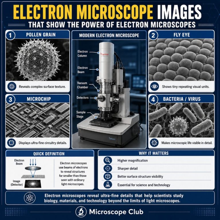
Electron microscope images reveal a world that visible light can never reach — individual atoms, flash-frozen viral proteins, and the claw of a mite clinging to a honeybee’s back. This guide explains how electron microscopes produce those images, what the color and scale bars actually mean, and how to read every picture in the gallery below with the same eye a microscopist brings to the instrument.
What an electron microscope is — and why it beats light

Electron microscopes are instruments that form images by firing a beam of accelerated electrons at a specimen rather than shining visible light on it. That single substitution — electrons for photons — is responsible for every performance leap. Electrons, when accelerated through tens of thousands of volts, carry a de Broglie wavelength that can fall below 0.003 nm, roughly 100,000 times shorter than a photon of green light. Because resolving power is fundamentally limited by wavelength, an electron microscope can resolve details that are physically invisible to any light microscope, no matter how well its glass lenses are made.
The practical result: the best light microscopes resolve features down to roughly 200 nm. The current world-record electron microscope — using a technique called electron ptychography — has resolved features at approximately 20 picometres (0.02 nm) — far smaller than a single atom, about a fifth of a hydrogen atom’s diameter — per a 2021 Cornell Chronicle report and confirmed independently by Guinness World Records. That is not marketing language; it is a measured, peer-reviewed result.
The tradeoff is that electrons cannot travel through air without scattering. The entire beam path, from the electron gun at the top of the column to the detector at the bottom, operates in a high vacuum. This has far-reaching consequences for sample preparation, as you will see below.
How an electron microscope works
The electron microscope column contains three core systems working in sequence:
- Electron gun. A heated tungsten filament or a field-emission tip strips electrons from the metal and accelerates them through a high-voltage field — typically 5 to 300 kV depending on the instrument type. The voltage controls the wavelength: higher voltage = shorter wavelength = higher potential resolution.
- Electromagnetic lenses. Instead of glass, electron microscopes use coils of wire carrying current. The magnetic field these coils produce bends the electron beam the same way glass bends light. Aberration correctors — stacked sets of multipole lenses — compensate for the beam distortions that would otherwise blur the image; they are the reason modern instruments can approach atomic resolution.
- Detectors. What gets detected depends on the instrument type. In a scanning electron microscope (SEM), a detector collects low-energy secondary electrons (SE) knocked off the specimen’s surface, or higher-energy backscattered electrons (BSE) that bounce back from within the sample. In a transmission electron microscope (TEM), electrons that pass through a thinned sample are collected below it and form an image on a camera.
The four main types of electron microscope — compared
The original article named two types. The full modern family is wider, and one of them — cryo-EM — won the Nobel Prize in Chemistry in 2017.

| Type | What it detects | What you see | Typical uses | Gallery example here |
|---|---|---|---|---|
| SEM (Scanning Electron Microscope) |
Secondary & backscattered electrons reflected from the surface | Surface topography and texture; 3-D appearance; composition contrast on BSE mode | Insects, pollen, fractured metal surfaces, semiconductor inspection, forensics | Whitetop gall mite; Varroa destructor; iron crystals from the moon; blood cells (colorized SEM) |
| TEM (Transmission Electron Microscope) |
Electrons transmitted through a ultra-thin slice of specimen | Internal structure — organelles, crystal planes, lattice defects, viral capsids | Cell biology, virology, materials science, nanoparticle characterization | Pollen wall cross-section; organic chemical reaction frame |
| STEM (Scanning Transmission Electron Microscope) |
Transmitted electrons from a scanned focused probe | Atomic columns; annular dark-field images show heavy-atom positions with exceptional contrast | Atom-by-atom materials characterization, catalyst research, semiconductor defect analysis | The 20 pm ptychography record image (Cornell, 2021) is a STEM/ptychography result |
| Cryo-EM (Cryogenic Electron Microscopy) |
Transmitted electrons through a vitrified (glass-like frozen) biological sample | 3-D structure of proteins, viruses, and ribosomes at near-atomic resolution, without staining or dehydration artifacts | Structural biology, drug target determination, vaccine design | No gallery image here — see COVID-19 spike protein maps for a famous example |
| FIB-SEM (Focused Ion Beam + SEM) |
SEM imaging combined with a focused gallium-ion beam for milling | Serial cross-sections through a volume → 3-D reconstructions of cells or circuit structures | Semiconductor failure analysis, 3-D connectomics, site-specific TEM sample preparation | — |
For a deeper comparison of the two most commonly encountered types, see our guide to scanning vs transmission electron microscopes. For context on how these instruments stack up against optical alternatives, the page on advantages and disadvantages of electron microscopes is a useful companion read.
Why electron microscope images are black and white — and when color is added
Electron microscope images are natively grayscale. SEM detectors measure how many secondary or backscattered electrons arrive per pixel; TEM detectors measure transmitted-electron intensity. Neither process captures wavelengths of visible light, so there is no color information in the raw data — just intensity values from dark to bright, rendered as a grayscale map.
Every color you see in famous EM images — the vivid orange of a Varroa mite, the electric-blue blood cells in a science magazine — is false color, added by researchers or illustrators afterward in image processing software. False color is not deceptive; it is a labeling tool. Different colors are assigned to different structural regions or elemental signals (from an EDX/EDS detector) so that a viewer can distinguish them at a glance. When you see a colorized EM image, the colors communicate “these regions are structurally distinct,” not “this is what it would look like if you could see it with your eyes.”

The gallery below identifies which images carry false color and what each color indicates.
How to read any electron microscope image
Apply this four-point checklist to every EM image you encounter, including the ones in this gallery:
- Identify the type — SEM or TEM? Surface relief with a sculptural, three-dimensional look = SEM. A flat slice showing internal structure, organelles, or crystal planes = TEM. STEM images resemble TEM but often show bright dots on a dark background (annular dark-field) corresponding to heavy-atom columns.
- Treat color as a label, not a photograph. The color is not real. Ask: what did the researcher use color to distinguish — surface regions, elemental composition, different cell types? If the image credit does not explain the coloring, treat the image as informational illustration, not literal representation.
- Find the scale bar. Published EM images always include a scale bar — a short line labeled with a physical distance (e.g., “1 µm” or “500 nm”). The magnification number printed on the image is meaningless without knowing the output size; the scale bar is the only reliable size reference. Images in this gallery that lack visible scale bars are cropped or reproduced from their original publication — refer to the credited source for the original scale data.
- Ask what the light microscope could not show. The maximum resolution of a light microscope is ~200 nm. Anything smaller than that — individual viral particles (~100 nm), ribosome subunits (~25 nm), atomic columns (<1 nm) — is electron-microscope-only territory. Asking this question converts the image from a visual novelty into a scientific claim.
Sample preparation — the skill that makes or breaks the image

Sample preparation is where electron microscopy expertise actually lives. The vacuum inside the column destroys living specimens and collapses hydrated biological tissue, so every sample must be either dehydrated and dried, coated, cryogenically preserved, or thinned to electron transparency before it enters the instrument.
Sputter coating (SEM)
Non-conductive specimens — insects, plant material, polymers, ceramics — accumulate electrostatic charge under the electron beam and produce bright, washed-out images. The fix is sputter coating: a thin conductive layer of gold, platinum, or chromium, typically 5–10 nm thick, is deposited onto the specimen surface under argon plasma, as documented by Leica Microsystems. The metal conducts charge away from the surface without masking the fine structural details the researcher wants to image.
Critical-point drying (SEM)
Biological material is mostly water. Drying it in air causes surface tension to collapse delicate structures as the water evaporates. Critical-point drying replaces the water with liquid CO₂, then takes the CO₂ past its critical point (31 °C, 74 bar) where the liquid and gas phases are identical — there is no surface tension to collapse anything. The specimen emerges dry, structurally intact, and ready to coat.
Cryo-fixation (cryo-EM)
Cryo-EM sidesteps both problems. A thin film of the specimen — often a protein solution or a cell suspension — is spread on a holey carbon grid and plunged into liquid ethane at −183 °C so rapidly (milliseconds) that water molecules do not have time to form ice crystals. They solidify into vitreous ice, a glass-like amorphous solid that preserves the biological structure in its native, hydrated state at atomic resolution. This technique, developed by Jacques Dubochet (2017 Nobel Prize in Chemistry), is why cryo-EM can now determine protein structures that would otherwise require large, well-ordered crystals for X-ray diffraction.
TEM sectioning
TEM requires the specimen to be thin enough for electrons to pass through — typically 50–100 nm for biological samples, thinner still for hard materials. Biological specimens are chemically fixed, embedded in resin, and cut with a diamond knife on an ultramicrotome into sections so thin they float on water. The pollen wall image in the gallery below shows exactly this kind of cross-sectional preparation.
Key facts about electron microscopes
Seven centuries of optical science underpin the electron microscope. The first true magnifying lenses date to the 13th century; the compound microscope appeared around the 1590s. The electron microscope is the most recent and most powerful development in that lineage.
- Ernst Ruska and Max Knoll built the first electron-lens apparatus in 1931 — a proof of concept that achieved low magnification. By 1933, Ruska’s improved instrument surpassed the resolution limit of the light microscope for the first time. Ernst Ruska received the Nobel Prize in Physics in 1986 for this work.
- The current world-record resolution — approximately 20 picometres — was achieved in 2021 by David Muller’s team at Cornell University using electron ptychography, a computational reconstruction technique applied to STEM data. That is far smaller than a single atom — about a fifth of a hydrogen atom’s diameter (a hydrogen atom has a radius of ~53 pm, giving it a diameter of ~106 pm).
- Cryo-electron microscopy won the 2017 Nobel Prize in Chemistry (Jacques Dubochet, Joachim Frank, Richard Henderson) for enabling near-atomic-resolution imaging of biological molecules in their native state.
- Modern electron microscopes from Thermo Fisher Scientific (the Titan Themis), JEOL (the ARM-300F), and Nion (the Hermes STEM) incorporate aberration correctors that push resolution into the sub-50-pm range for routine materials work — not a single-vendor achievement but a field-wide advance.
- For more on the instruments that hold the highest magnification records, see our guide to which microscope achieves the highest magnification.
Electron microscope images — gallery and analysis
The images below span SEM, cryo-SEM, and TEM techniques and cover specimens from parasitic mites to lunar rock. Each caption explains which instrument type was used, why that type was chosen, what the color indicates, and what the structure reveals that a light microscope could not.
Flora and fauna

Insects, mites, parasites, and plant structures are natural targets for SEM because the technique excels at surface topography at scales too small for any camera lens. The sculptural, three-dimensional appearance of SEM images comes from the way secondary electrons escape preferentially from raised edges and fine features — these regions appear bright, giving the image its striking depth even though the output is a 2-D intensity map. All color on the images below is false color added in post-processing.
Internal structure of a pollen grain

This image shows a cross-section of a pollen grain wall prepared by acetolysis — a chemical treatment using acetic anhydride and sulfuric acid that digests the pollenkit (the oily outer coating) and removes cytoplasm, leaving only the tough sporopollenin skeleton of the wall. What remains is an extraordinarily stable biopolymer that has survived in the fossil record for hundreds of millions of years. The layered architecture visible here — the thickened aperture regions and the reticulate (net-like) surface pattern — is unique to each plant species, which is why pollen analysis (palynology) can identify ancient plant communities from sediment cores.
A light microscope can show you the overall shape of a pollen grain, but the sub-micrometre wall ultrastructure in this image is entirely below the light microscope’s resolution limit. The fine surface detail is nanometre-scale — only an electron beam can map it.
Image taken by Louisa Howard from Dartmouth College’s E.M. Facility
Whitetop gall mite (Aceria drabae)

This SEM image shows Aceria drabae, the whitetop gall mite — an eriophyid mite so small it is invisible to the naked eye. The specimen was imaged by SEM because eriophyid mites are less than 200 µm long; photographing them with a light microscope gives a blurred, featureless silhouette, while SEM resolves the annulated (ring-segmented) cuticle and the paired chelicerae used to pierce plant tissue.
Aceria drabae is an approved biological control agent for hoary cress (Lepidium draba), an invasive Eurasian weed that displaces native plant communities across western North America. The mite feeds inside developing buds and causes stunting and galling that suppress both seed production and vegetative spread. Following its first global field release in Montana in 2019, the USDA APHIS approved additional Wyoming releases in 2022; by 2024, the mite had been released at approximately 26 sites and established at roughly 70% of them, according to Montana State University Extension (2025).
Image taken by Annie de Meij from Montana State University
Varroa destructor on a honeybee

Varroa destructor is the most damaging ectoparasite of managed honeybee colonies worldwide. This image was captured on a low-temperature SEM (also called cryo-SEM), a variant that chills the specimen with liquid nitrogen before it enters the vacuum chamber rather than chemically dehydrating it. Cryo-SEM preserves the natural surface texture of both the mite and the bee’s cuticle — the bristles, leg joints, and inter-segment membranes are all in their hydrated, life-like configuration rather than collapsed and contracted from chemical fixation.
The image rewards careful reading. The mite’s broad, flattened body — an adaptation for clinging between abdominal segments — is visible against the bee’s similarly tough exoskeleton. The mite’s eight legs and mouth parts are identifiable at SEM resolution; all of this is below the threshold of what a light microscope could show cleanly at this working distance.
This is an excellent depiction of parasitism at the microscopic scale, and one of the most widely reproduced SEM images in entomology.
Image taken by Erbe and Pooley from the US Department of Agriculture’s Agriculture Research Service
Cells and compounds

Biological cells sit at an interesting resolution boundary: the largest organelles (mitochondria, nuclei) can be seen at the edge of a light microscope’s capability, but their internal membranes, surface receptors, and interactions with pathogens require electron resolution. The two images below illustrate both SEM and TEM approaches to cellular imaging, plus one example of live chemistry captured on film inside a TEM column.
Human red blood cells (false-color SEM)

Red blood cells — erythrocytes — are approximately 6–8 µm in diameter and carry no nucleus, which makes them unusual among human cells and visible under a light microscope. But this image is SEM, not light microscopy, and the difference is stark. The biconcave disc shape that gives erythrocytes their characteristic flexible, oxygen-carrying geometry is rendered here in sculptural three-dimensional relief. The red color is false: native SEM output is grayscale; color was applied in post-processing to distinguish cell types and aid visual communication.
SEM imaging of blood cells is used in diagnostic research to detect morphological abnormalities — misshapen cells (echinocytes, sickle cells) that signal disease states — at a resolution that light microscopy cannot match. This image also illustrates how SEM post-processing can be automated to colorize and three-dimensionally render the intensity data, turning a monochrome map into an immediately intuitive anatomical illustration.
Image taken by Christophe Mignot from Cambridge University
Organic chemical reaction captured in a TEM

This frame was extracted from a real-time TEM recording of a carbon–sulfur bond formation reaction. The molecules — introduced to the TEM specimen space using a nanoscale reaction vessel — undergo bond formation under the electron beam, and the atomic-scale rearrangements are recorded as a sequence of images. What you are looking at is not a simulation or a computer-generated model: it is a direct electron-microscope image of individual molecules undergoing a chemical reaction.
This kind of in-situ TEM — where reactions, phase transitions, or crystal growth are observed directly inside the instrument — represents one of the frontier applications of electron microscopy. It is only possible because TEM operates at the sub-nanometre scale where individual molecular bonds are resolvable. For context on imaging individual atoms, this falls into the same resolution tier.
Inorganic material
Inorganic specimens — metals, minerals, crystals, ceramics, semiconductor devices — are among the most natural fits for SEM and TEM. They are already dry, frequently conductive, and do not degrade under the electron beam the way biological tissue does. The analytical power of SEM on inorganic material is especially strong when combined with energy-dispersive X-ray spectroscopy (EDX/EDS), which maps the elemental composition of each pixel alongside the structural image.
Iron crystals from the Moon

This SEM image shows iron crystals grown on a fragment of lunar rock collected during the Apollo 15 mission at the Hadley-Apennino landing site on November 10, 1972. The crystals grew slowly in the near-vacuum of the lunar surface over billions of years, and their near-perfect geometric form reflects exactly that unhurried, disturbance-free growth environment. On Earth, atmospheric oxidation, humidity, and thermal cycling would disrupt crystal growth and introduce defects; on the Moon, none of those factors operate.
Planetary scientists use SEM imaging of Apollo samples to characterize the mineralogy, grain size, and surface texture of lunar soils — information that constrains models of the Moon’s volcanic history and space-weathering environment. The SEM’s ability to image conducting metallic crystals directly, without coating, and to map elemental composition simultaneously via EDX, makes it the instrument of choice for this kind of geological work.
Image taken by NASA on November 10, 1972 from the Apollo 15 Hadley-Apennino lunar landing site
What electron microscopy has enabled — key discoveries
Electron microscopes have produced some of the most consequential scientific images in history. A short list of what would not exist without them:
- Viral structure. The detailed capsid architecture of viruses — including SARS-CoV-2 — is mapped by cryo-EM. Without it, rational vaccine design would rely on lower-resolution techniques that miss the binding sites that antibodies must target.
- Semiconductor manufacturing. Every node shrink in microchip fabrication — from 10 nm to 3 nm to sub-2 nm — is qualified and inspected using SEM and TEM. The transistor gates in a modern CPU are smaller than many proteins; there is no other way to verify they were formed correctly.
- Materials science. Grain boundary structure, dislocation density, and precipitate morphology in engineering alloys are all TEM/STEM measurements. The strength of jet turbine blades, the corrosion resistance of stainless steel, and the fatigue life of aerospace components depend on this data.
- Atomic manipulation. Imaging individual atoms at sub-50 pm resolution in an aberration-corrected STEM is now routine at university core facilities. The ability to identify which atom occupies which lattice site directly enables the design of quantum materials, catalysts, and next-generation battery electrodes. Any “manipulation” claim should be anchored to specific, measured results — the Cornell ptychography achievement (20 pm, 2021) is the current benchmark.
Who uses electron microscopes — and how to access one
Electron microscopes are not consumer instruments. A research-grade aberration-corrected STEM runs between $3 million and $7 million USD; even a basic tabletop SEM suitable for educational use starts around $70,000. As a result, access is almost always institutional:
- University core facilities. Most research universities operate shared-use electron microscopy labs — often called “EM core facilities” or “materials characterization labs” — that are open to external researchers on a fee-per-hour basis. This is the most practical route for academic researchers and graduate students. Search “[your university] electron microscopy facility” or check the directory maintained by the Microscopy Society of America.
- National laboratories. Facilities like the DOE Office of Science user facilities (Argonne, Oak Ridge, Brookhaven) house some of the most advanced instruments in the world and accept proposals from researchers globally on a competitive but free-at-point-of-use basis.
- Industrial quality control labs. Semiconductor fabs, aerospace manufacturers, pharmaceutical companies, and materials suppliers operate in-house EM labs for production inspection and failure analysis. These are not publicly accessible but represent the largest installed base of instruments globally.
- Tabletop SEMs. Benchtop instruments (Hitachi TM Series, Thermo Fisher Phenom, Zeiss EVO compact) bring basic SEM capability to smaller labs, college teaching environments, and some industrial QC settings at a price point comparable to a high-end analytical balance.
For a broader view of which instrument is right for which application, the comparison of light microscope vs electron microscope covers the practical tradeoffs in detail.
Electron microscope images — video
Frequently asked questions
Can electron microscopes see in color?
No. Electron microscopes detect electrons, not photons, so the raw output is always grayscale — a map of electron intensity, not wavelength. All color in electron microscope images is false color, added by researchers in image processing software to distinguish structural regions, elemental composition zones, or different specimen types. The color choice is arbitrary; the same image could be published in different color schemes by different labs.
What is the difference between SEM and TEM?
SEM (scanning electron microscope) scans a focused beam across the specimen surface and collects electrons that bounce off or are knocked out; it images surface topography and, in backscattered mode, surface composition. TEM (transmission electron microscope) fires a broader beam through an ultra-thin specimen slice and images the transmitted electrons below; it images internal structure. For a full breakdown, see the dedicated scanning vs transmission electron microscope comparison.
How much does an electron microscope cost, and who can use one?
Basic tabletop SEMs start around $70,000; research-grade aberration-corrected STEMs cost $3–7 million. Most researchers access them through university core facilities (fee per hour) or national laboratory user programs. Hobbyists can occasionally access community lab instruments through maker spaces or via university open-house programs, but home use is not practical.
What is the highest resolution of an electron microscope?
The current world record is approximately 20 picometres (0.02 nm), set in 2021 by David Muller’s team at Cornell University using electron ptychography on a STEM instrument. For comparison, a hydrogen atom is about 53 pm in radius. Routine aberration-corrected STEM imaging in university facilities typically resolves features in the 50–100 pm range — still easily atomic resolution.
How are samples prepared for an electron microscope?
Preparation depends on the instrument and specimen. SEM of biological material typically requires chemical fixation, dehydration (critical-point drying), and sputter coating with a thin conductive metal layer (5–10 nm of gold or platinum). TEM requires slicing the specimen to 50–100 nm thickness with a diamond-knife ultramicrotome. Cryo-EM plunge-freezes the specimen in liquid ethane to preserve it in vitreous ice without chemical treatment.
Why do samples have to be coated before SEM?
Non-conductive samples — most biological material, polymers, ceramics — accumulate electrostatic charge under the electron beam because they cannot conduct the charge away. This charging produces bright artifacts that obscure surface detail and can damage the specimen. Sputter coating deposits a thin (5–10 nm) conductive metal layer that dissipates the charge to ground, allowing a clean image to be formed.
What is cryo-electron microscopy?
Cryo-EM is a TEM technique in which the specimen — typically a protein solution, virus suspension, or cell — is flash-frozen in liquid ethane so rapidly that the water forms vitreous (glassy) ice rather than crystalline ice. Vitreous ice does not form the large ice crystals that would destroy biological structure, so the specimen is preserved in its native, hydrated state. Computational methods then reconstruct a 3-D structure from thousands of 2-D projection images taken at different angles. Cryo-EM won the 2017 Nobel Prize in Chemistry and is now the primary tool for determining protein structures that resist crystallization — including the spike proteins of coronaviruses.
Who invented the electron microscope?
Ernst Ruska (physicist) and Max Knoll (electrical engineer) built the first electron-lens apparatus in 1931 as a proof of concept at the Technische Hochschule Berlin. By 1933, Ruska’s improved instrument resolved detail finer than the best light microscope of the time — the first time this barrier had been crossed. Ernst Ruska received the Nobel Prize in Physics in 1986 for his invention of the electron microscope.
Originally posted 2020-04-13 07:06:59.