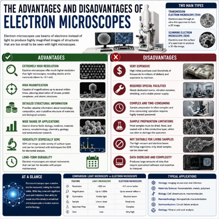
The electron microscope is the most powerful imaging tool ever routinely deployed in a laboratory — a device precise enough to resolve the space between neighboring atoms in a crystal lattice, or trace the folds of a protein no crystallographer has ever crystallized. The jump from a light microscope to an electron microscope isn’t incremental; it’s a leap of roughly a thousand to one in resolving power. That gap is why electron microscopes sit at the center of some of the most significant scientific discoveries of the past century, from the three-dimensional structure of viruses to the atomic architecture of next-generation battery materials.
Advantages of electron microscopes
As one of the most advanced types of microscopes ever developed, an electron microscope offers capabilities no other instrument can replicate. Each advantage below traces back to the same fundamental physics: electrons, focused by magnetic lenses, carry far more resolving power than photons ever can.
High magnification

One of the most striking things about working with an electron microscope for the first time is the scale compression it delivers. You load a specimen you could lose between your fingers, and the microscope returns an image where individual atoms register as visible intensity peaks in the data — real positions of real atoms, not models.
Scanning electron microscopes (SEMs) operate across a range of roughly 10× to 1,000,000×; transmission electron microscopes (TEMs) can exceed 10,000,000× when resolving atomic detail. Older figures citing “up to 500,000×” reflect SEM performance, not TEM capability. For comparison, the practical ceiling of a light microscope sits around 1,500× — limited by the wavelength of visible light itself. Beyond that you get a brighter blur, not more detail.
What makes this possible: instead of photons, the electron microscope fires a beam of accelerated electrons through or across the specimen, then focuses them with electromagnetic lenses shaped by precisely controlled magnetic fields — the same optical principle as glass lenses, but adjustable by varying current rather than grinding a new element. Electron optics are tunable in ways glass never will be.
See also: which microscope achieves the highest magnification

High resolution
Magnification without resolution is just a blurry enlargement. Resolution — the ability to distinguish two features that sit very close together — is where electron microscopes truly separate themselves from every other instrument class.
Modern TEMs achieve sub-ångström resolution. Routine high-resolution TEM sits around 0.5 Å point resolution; aberration-corrected scanning TEM (STEM) pushes below 50 pm; and a 2024 ptychography study at the University of Illinois achieved a record 0.44 Å in an uncorrected instrument Science, 2024. To put that in scale: a human hair is roughly 80,000 nm wide — the best electron microscopes resolve structures a billion times smaller.
The physics is fundamental. Resolving power is constrained by wavelength. Electrons accelerated at 100 keV carry a de Broglie wavelength of approximately 0.0037 nm — tens of thousands of times shorter than visible light (400–700 nm). The shorter the wavelength, the finer the detail you can resolve. Light microscopy is fundamentally limited to approximately 200 nm by this same principle; an electron microscope doesn’t improve on that limit, it demolishes it by three orders of magnitude.

See also: how microscope resolution works
SEM vs. TEM — two instruments with different strengths
The single most important thing to understand about electron microscopes is that “electron microscope” is not one instrument. The two dominant types — the scanning electron microscope (SEM) and the transmission electron microscope (TEM) — have entirely different operating principles, and therefore different strengths, limitations, and use cases.
SEM scans a focused electron beam across the specimen’s surface and collects the secondary and backscattered electrons that emerge. The result is a topographic image of the surface with a striking pseudo-3D quality — depth, shadow, and texture that can make a pollen grain look like a sculpture. SEMs handle relatively large, bulky samples, require less extreme preparation than TEM, and are considerably more affordable and accessible. Resolution on a high-performance SEM reaches around 0.5–1 nm. The limitation: you see only the surface.
TEM fires electrons straight through an ultra-thin specimen slice — typically under 100 nm thick — and builds an image from the transmitted and diffracted electrons. TEM reveals crystal lattices, grain boundaries, internal biological architecture, and atomic-scale defects in stunning detail. The trade-off: specimens must be precision-sliced to near-transparency, the field of view is extremely small, and the instruments are significantly more expensive and demanding to operate.
See also: transmission vs. scanning electron microscope — a full comparison
Versatility of use
The combination of extreme resolution and adaptable specimen handling is what made electron microscopes indispensable across such a wide range of disciplines. Real-world examples make the breadth concrete:
- Semiconductor manufacturing: SEM is used daily for quality control and failure analysis — inspecting for voids, shorts, and deposition irregularities in transistor features too small to see any other way. At 5 nm node and below, it is the primary metrology tool.
- Battery and catalyst R&D: TEM and STEM reveal how nanoparticles restructure at the atomic level during charge cycles or catalytic reactions — information that directly informs material design.
- Structural biology and vaccine development: Cryo-EM determined the three-dimensional structure of the SARS-CoV-2 spike protein within weeks of the viral sequence being published, directly enabling mRNA vaccine design.
- Forensic science and materials failure: SEM identifies particulates, fracture surfaces, corrosion morphology, and trace contaminants that remain completely invisible to optical instruments.
- Geology and mineralogy: SEM with EDS maps elemental distribution across mineral grains, identifying phase boundaries and alteration chemistry that thin-section petrography cannot resolve.
Whichever type of material you need to analyze — organic, inorganic, crystalline, amorphous, hard, or soft — there is an electron microscope configuration suited to the task. This breadth of application is why the technology became established in fields ranging from pure academic research to high-volume industrial quality control.
Compatibility with other analytical technologies

What makes a modern electron microscope research station genuinely powerful isn’t the imaging alone — it’s the suite of analytical techniques that run simultaneously, turning a picture into a periodic-table map of the material.
Key coupled techniques include:
- EDS/EDX (Energy-Dispersive X-ray Spectroscopy): the electron beam ejects characteristic X-rays from the specimen that identify which elements are present and where. The result is an elemental composition map overlaid on the image — invaluable for materials science, semiconductor analysis, and failure investigation.
- EELS (Electron Energy Loss Spectroscopy): measures how much energy electrons lose passing through the sample, revealing elemental composition, electronic structure, and bonding state. More sensitive than EDS for light elements such as lithium, boron, and carbon.
- FIB-SEM (Focused Ion Beam + SEM): a gallium ion beam mills material away slice by slice while the SEM images each newly exposed surface, producing a true 3D reconstruction of the specimen’s interior volume.
- Electron tomography: collects TEM images at multiple tilt angles and computationally reconstructs a 3D volume from the projection series — the electron microscopy equivalent of a CT scan.
- STEM (Scanning Transmission Electron Microscopy): combines TEM-class resolution with a scanned probe geometry, enabling atomic-column imaging and simultaneous EDS/EELS mapping at the sub-ångström scale.
One important clarification on a common misconception: standard EM images are inherently greyscale. Electrons carry no wavelength or color information. Any color you see in a published electron microscope image is false-color applied computationally in post-processing to highlight features, distinguish phases, or aid visualization. Similarly, “3D” imaging is not a native output — it comes from SEM’s topographic surface contrast, FIB-SEM serial sectioning, or electron tomography reconstruction. These are powerful add-ons, not built-in capabilities of the base instrument.
Cryo-EM — imaging biomolecules in their natural state
One of the most transformative advances in the history of electron microscopy was the development of cryo-electron microscopy — cryo-EM. The technique earned the 2017 Nobel Prize in Chemistry for Jacques Dubochet, Joachim Frank, and Richard Henderson, awarded “for developing cryo-electron microscopy for the high-resolution structure determination of biomolecules in solution” Nobel Prize in Chemistry 2017.
The core problem cryo-EM solved: conventional TEM requires specimens to be dehydrated and chemically fixed, which destroys soft biological structures. High-resolution structural work previously required growing protein crystals — a slow, difficult, and often impossible process for membrane proteins and large complexes. Cryo-EM sidesteps both constraints.
In cryo-EM, the protein or virus sample is applied to a grid and plunge-frozen at millisecond speed into liquid ethane — not liquid nitrogen, which is a critical distinction. Liquid nitrogen causes the Leidenfrost effect: it boils on contact with the warm sample, forming an insulating vapor layer that slows cooling and allows ice crystals to form, destroying biological structure. Liquid ethane has higher heat capacity and doesn’t form this vapor layer, cooling fast enough to trap water in an amorphous, glassy state. The frozen molecules are structurally preserved in near-native conditions, without crystallization or chemical fixation.
The practical result is extraordinary: when the SARS-CoV-2 sequence was published in January 2020, cryo-EM solved the three-dimensional structure of its spike protein in approximately twelve days — a result that would have taken years by X-ray crystallography, if it had been achievable at all. That structure directly informed the design of mRNA vaccines that went to clinical trial the same year.
Disadvantages of electron microscopes
With those capabilities come real constraints — some practical, some fundamental to the physics. Understanding the limitations is as important as knowing the strengths, particularly when choosing the right tool for a given question.
Size, cost, and housing requirements
The most immediate obstacle for most institutions is practical: electron microscopes are large, expensive, and demanding in their facility requirements.
A research-grade TEM occupies a dedicated room and typically costs $1–3 million for the instrument alone; some aberration-corrected instruments exceed $10 million. The building itself must provide vibration isolation, acoustic damping, electromagnetic shielding, and thermal stability. The most demanding ultra-high-resolution TEMs sit on 40-ton concrete foundations sunk several meters underground — not primarily for magnetic-field cancellation, but for vibration isolation. At sub-ångström resolution, a footstep in an adjacent corridor registers as measurable noise. Most routine SEMs sit in ordinary laboratories, but even these require stable electrical supply and magnetic-field control.
That said, this picture has become less absolute. Benchtop desktop SEMs are now commercially available — instruments small enough for a laboratory bench, operable at low vacuum, with resolutions in the 5–20 nm range. They trade performance for accessibility and cost, but they have brought electron microscopy into labs, educational settings, and smaller R&D environments that previously had no access.
See also: how much an electron microscope costs
Specimen environment — the vacuum requirement


Every conventional electron microscope operates at high vacuum — typically 10⁻⁴ to 10⁻⁷ Pa inside the column. This isn’t a design choice; it’s physically required. An electron beam traveling even a few centimeters through air at atmospheric pressure is completely scattered by gas molecules before reaching the specimen. Vacuum is not optional.
For biological and hydrated specimens, this creates an obvious problem: most biological material is primarily water, which evaporates immediately under vacuum. Standard solutions include dehydration prior to loading, or cryo-freezing to prevent sublimation.
Environmental SEM (ESEM) offers a partial workaround. ESEM operates at higher pressures (up to a few thousand Pa) in the specimen chamber, allowing hydrated, non-conductive, or even liquid samples to be imaged at reduced resolution and contrast. ESEM is particularly useful for food science, pharmaceutical materials, and geological samples where conventional dehydration would alter the very structure being studied.
A consequence worth stating clearly: living specimens cannot be imaged in a conventional electron microscope. The vacuum alone is lethal, and the electron beam causes additional radiation damage. Cryo-EM preserves structure brilliantly, but frozen is not alive. For imaging living cells and dynamic biological processes, light microscopy — particularly fluorescence and confocal variants — remains the only viable approach.
Sample preparation — the hidden time cost
Sample preparation is mentioned as a brief footnote in many introductions to electron microscopy. In practice, it is often the most time-consuming, skill-intensive, and error-prone part of the entire workflow.
For biological TEM, a standard preparation involves: chemical fixation in glutaraldehyde, dehydration through a graded ethanol series, resin infiltration and curing, ultra-thin sectioning on an ultramicrotome targeting 60–90 nm sections (thinner than many viruses), heavy-metal staining with uranyl acetate and lead citrate for contrast, and mounting on a copper TEM grid. From biopsy to grid, this process typically takes two to three days. A section that tears, folds, or picks up a contaminating particle means starting over at that step. Every electron microscopist accumulates a personal vocabulary of disasters — sections that curl on the knife, grids that drop grid-side-down, stain precipitate that obscures the region of interest.
For SEM, preparation is shorter, but non-conductive specimens must be coated with a thin conductive layer — typically gold, gold/palladium, or carbon, deposited by sputter-coating — to prevent charge accumulation. Uncoated non-conductors glow with a white charging artifact that obscures all surface detail. Beginner mistake: loading an uncoated polymer and wondering why the image looks overexposed.
Cryo-EM vitrification adds its own demands: the protein solution must be applied at exactly the right concentration, blotted to a thin film of 3–100 nm, and plunge-frozen within milliseconds. Too thick — electrons can’t penetrate. Too thin — the sample dries before freezing. The right condition is found empirically, usually over many discarded grids.
Radiation and beam damage
A significant disadvantage the original article omits: the electron beam that creates the image also damages the specimen.
High-energy electrons transfer energy to the material they pass through. For robust inorganic specimens — metals, semiconductors, minerals — this is often negligible. For biological and organic specimens, radiation damage is a fundamental constraint. The beam breaks chemical bonds, causes radiolysis (radiation-induced decomposition), and progressively destroys the structure being imaged. The same electrons that produce the image are simultaneously altering what you are trying to measure.
This is a primary reason cryo-EM uses low-dose imaging protocols — collecting images at the minimum electron dose that still yields a usable signal before the molecule is too damaged to interpret. It is also why conventional TEM of biological material almost always works on dead, fixed, stained specimens rather than anything approaching a natural state.
For materials science, beam damage is relevant when studying soft polymers, beam-sensitive ceramics, zeolites, and certain catalysts, where the act of imaging induces structural changes in the specimen under study — a version of the observer effect made very literal.
Electron microscope vs. light microscope — key differences at a glance
Understanding where electron microscopy excels and where light microscopy is still the better choice requires a direct comparison. The two technologies are complementary, not competitive.
| Feature | Light microscope | Electron microscope |
|---|---|---|
| Practical resolution limit | ~200 nm | <0.1 nm (TEM) / ~0.5 nm (SEM) |
| Maximum magnification | ~1,500× | 1,000,000×+ (TEM: 10,000,000×) |
| Specimen state | Live or fixed | Fixed, dehydrated, or cryo-frozen |
| Color | Natural or fluorescent | Greyscale (false-color in post-processing) |
| Sample preparation | Minimal to moderate | Moderate (SEM) to extensive (TEM/cryo-EM) |
| Vacuum required | No | Yes (standard); partial exception: ESEM |
| Approximate cost range | $500 – $100,000 | $10,000 (desktop SEM) – $10M+ (TEM) |
| Best suited for | Live cells, dynamic processes, large fields of view | Nanoscale structures, materials analysis, atomic detail |
See also: how electron microscopes compare to light microscopes
Frequently asked questions
What are the main advantages of an electron microscope over a light microscope?
Resolution and magnification. A light microscope cannot resolve features smaller than about 200 nm — a hard limit imposed by the wavelength of visible light. Electron microscopes use electron beams with wavelengths tens of thousands of times shorter, enabling resolution down to 0.1 nm or below in modern TEM instruments. This allows scientists to see individual atoms, virus structures, crystal defects, and molecular machines that are completely invisible to light optics.
What is one disadvantage associated with electron microscopes?
The most commonly cited disadvantage is sample preparation: specimens must be killed, dehydrated or cryo-frozen, and often sectioned or coated before imaging. Unlike light microscopy, you cannot observe a living cell in a conventional electron microscope. Additional practical disadvantages include cost, facility requirements, and radiation damage to sensitive specimens.
Why must electron microscope samples be in a vacuum?
Because electrons are scattered by gas molecules. An electron beam passing through even a few centimeters of air at atmospheric pressure would be completely deflected before reaching the specimen. High vacuum — typically 10⁻⁴ to 10⁻⁷ Pa — keeps the beam path clear from the electron gun to the specimen and detector. Environmental SEM (ESEM) operates at higher pressures as a partial exception, but standard instruments require high vacuum throughout the column.
Can electron microscopes see living cells?
No. Conventional electron microscopes require a vacuum that instantly kills any living organism, and the electron beam causes radiation damage that would further destroy biological structures. Cryo-EM preserves cells and molecules in a near-native frozen state with extraordinary structural detail, but frozen is not living. For imaging living, dynamic biological processes, fluorescence and confocal light microscopy remain the methods of choice.
Why are electron microscope images black and white?
Because electrons carry no wavelength or color information — color is a property of photons, not electrons. The EM detector records intensity (how many electrons arrived and where), producing a greyscale image. Any color seen in published EM images has been added computationally in post-processing, typically to highlight different structures, phases, or elemental regions. False-coloring is a visualization tool, not a measurement.
What is the difference between SEM and TEM?
SEM (scanning electron microscope) scans a beam across the specimen’s surface and images the electrons that bounce back, producing topographic surface images with pseudo-3D depth. TEM (transmission electron microscope) fires electrons through an ultra-thin specimen slice and images the transmitted electrons, revealing internal structure at atomic resolution. SEM is generally more accessible and handles larger samples; TEM offers far higher resolution but requires extensive specimen preparation and significantly greater cost.
How much does an electron microscope cost?
The range is enormous. Entry-level desktop SEMs start around $10,000–$50,000. Mid-range research SEMs run $100,000–$500,000. High-end field-emission SEMs and entry TEM instruments cost $500,000–$2 million. Aberration-corrected STEM instruments used for atomic-resolution materials science exceed $5–10 million. Factor in facility preparation, maintenance contracts, and consumables, and the total cost of ownership for a high-end TEM installation can easily reach $15–20 million over the instrument’s operational life. See: how much an electron microscope costs.
Conclusion
Electron microscopes are uniquely powerful imaging tools — capable of resolving individual atoms, mapping elemental composition, and revealing the three-dimensional architecture of biomolecules that no other technique can reach. The 2017 Nobel Prize for cryo-EM is the clearest signal yet that this technology’s impact continues to expand rather than plateau. The constraints are real: cost, facility demands, vacuum requirements, complex sample preparation, and beam damage all limit where and how electron microscopy can be applied. But for questions that require nanoscale or atomic-scale answers, no alternative exists. Scientists and engineers continue to push the boundaries of what these instruments can do — benchtop SEMs are making the technology more accessible, aberration correction is making TEM sharper than ever, and cryo-EM is rewriting structural biology. The electron microscope is not a solved technology; it is still being invented.
See also: electron microscope images