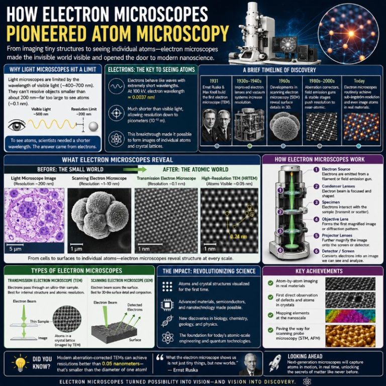
For most of human history, the atom was a philosophical concept — matter’s smallest theorized unit, invisible by definition. That changed in 1931, when a pair of German scientists aimed a beam of electrons at a thin specimen and produced an image no light microscope could ever rival. Today, we don’t just see atoms; we move them one by one, spell words with them, and use the images they produce to design drugs, semiconductors, and entirely new classes of materials.
Why electrons can see what light cannot
Every microscope’s resolution is limited by the wavelength of whatever it uses to illuminate a specimen. Visible light oscillates at wavelengths between roughly 400 and 700 nanometers, and the Abbe diffraction limit means no light microscope — however finely engineered — can resolve details finer than about 200 nm (University of Utah Advanced Microscopy). That is good enough to see a cell nucleus or a mitochondrion but nowhere near sufficient to resolve an atom, which measures roughly 0.1–0.3 nm across.
Electrons change the equation entirely. When accelerated through a high voltage, an electron’s de Broglie wavelength drops to just a few picometers — thousands of times shorter than visible light. That is the core reason electron microscopes can image atoms while optical microscopes cannot: it is not engineering cleverness, it is physics.

What microscope can see atoms?
The short answer is electron microscopes — and, for manipulating individual atoms, scanning probe microscopes. The longer answer depends on what you mean by “see.”
In a modern aberration-corrected scanning transmission electron microscope (STEM), individual atoms appear as bright spots against a dark field. The current world resolution record, set by Cornell’s Muller group using a technique called electron ptychography, is 0.39 ångströms — smaller than the diameter of a hydrogen atom (Cornell Chronicle, 2018). That is not a photograph in the conventional sense; it is a mathematical reconstruction from measured electron signals. The bright dots represent atomic columns projected along the beam direction — you are often looking end-on down a column of many atoms stacked in a crystal lattice, not at a single isolated atom floating in space. That honest caveat is worth holding onto: it does not diminish the achievement; it makes it more remarkable.
What is the purpose of an electron microscope?
When researchers at IBM first imaged graphene’s hexagonal lattice — six carbon atoms arranged in a perfect honeycomb ring, each C–C bond measuring 0.142 nm — they weren’t just taking a photograph. They were confirming the bond geometry that determines graphene’s extraordinary electrical conductivity. That is the deeper purpose of atom microscopy: seeing why a material behaves the way it does, written in the spatial arrangement of its atoms.

By imaging how atoms cluster, bond, and occasionally misbehave — a vacancy here, a substituted dopant atom there — researchers can connect atomic-scale structure directly to macroscopic properties like strength, conductivity, and catalytic activity. Materials that looked chemically identical could exhibit wildly different behaviors; atom-resolution imaging explained those differences and opened the door to deliberately engineering materials at the atomic scale.
What can you do with an electron microscope?
The capabilities go well beyond capturing a still image. Modern electron microscopes can:
- Map the chemical identity of each atom using energy-dispersive X-ray spectroscopy (EDS) or electron energy-loss spectroscopy (EELS) — so a single scan shows not just where atoms are but what element each one is.
- Track magnetic and electric fields inside a material by measuring the phase shift electrons accumulate as they pass through.
- Reconstruct three-dimensional models through electron tomography — rotating the specimen and combining dozens of 2D projections into a full 3D volume.
- Image specimens under real working conditions using in-situ stages: a catalyst particle while it is actively reacting, a battery electrode while it charges and discharges.
What materials can be imaged with an electron microscope?

Electron microscopes are remarkably versatile. Specimens studied include metals, ceramics, semiconductors, polymers, and biological tissue — fixed cells, thin-sectioned brain slices, viruses, and whole insects. In a scanning electron microscope, a common house ant fills the frame like an alien creature: each compound eye resolves as a mosaic of hexagonal lenses, the surface of each segment rippled with fine sensory hairs that no optical microscope could separate. What the SEM reveals that light microscopy obscures is surface texture at the nanometer scale — the difference between a polished and a corroded metal grain boundary, or the crystalline facets of a dust particle retrieved from space.

Organic and hydrated specimens present a challenge because electrons interact strongly with water. That drove the development of specialized techniques now considered mainstream: cryo-electron microscopy freezes biological samples in vitreous ice so rapidly that the water never forms damaging ice crystals, preserving the specimen in near-native state. It was this capability that earned the 2017 Nobel Prize in Chemistry for Jacques Dubochet, Joachim Frank, and Richard Henderson — cryo-EM had by then produced near-atomic-resolution structures of viruses and membrane proteins that crystallography could not access.
What are the applications of electron microscopy?
Fields that rely directly on electron and atom microscopy include:
- Semiconductor fabrication — verifying transistor dimensions now measured in a handful of atoms, detecting defects before a wafer ships.
- Materials research — understanding failure modes in alloys, ceramics, and composites at the grain level.
- Biology and structural biology — mapping protein complexes, resolving viral capsid structures used to design vaccines and antivirals.
- Pharmaceutical research — visualizing drug nanoparticles and lipid delivery systems for research into targeted therapies; contributions here are to the research phase, not clinical treatment.
- Forensics and geology — identifying mineral phases, gunshot residue particles, and trace materials.
- Nanotechnology — both observing and enabling manipulation at the atomic and molecular scale.
What is nanotechnology?
Nanotechnology is the study and application of matter at the atomic, molecular, and supramolecular scale — generally below 100 nm. It is inseparable from atom microscopy: you cannot engineer what you cannot see. Electron and scanning probe microscopes are simultaneously the observation tool and, in some configurations, the manipulation tool that makes nanotechnology possible.
How does an electron microscope work?
The fundamental mechanism is replacing photons with electrons. A high-voltage electron gun (typically using a field-emission tip or a tungsten filament cathode) fires a beam of electrons that is then shaped and focused by electromagnetic lenses — coils of wire that bend electron paths the way glass bends light. The focused beam strikes the specimen, and the signals generated — transmitted electrons, scattered electrons, secondary electrons, X-rays — are detected and processed into an image.
Resolution is not just about magnification. Modern aberration-corrected instruments use sophisticated multipole lens systems to compensate for spherical and chromatic aberrations that would otherwise blur the image. That correction is what pushed resolution below 1 Å, and ultimately to the 0.39 Å record. The highest magnification achievable on advanced STEM instruments exceeds 10,000,000×, but resolution — the ability to distinguish two adjacent atoms — is the meaningful metric to quote.
How the microscope works in detail depends on which type you are using.
Electron microscope vs compound microscope
The difference comes down to physics, not engineering. A compound light microscope uses visible light, bounded by the Abbe diffraction limit at roughly 200 nm. You can push magnification higher — some microscopes go to 2000× — but beyond about 1000–1500× you are producing “empty magnification”: the image gets bigger but no new detail appears, because the light simply cannot carry finer information. That is why light microscopes are perfect for cells but cannot resolve viruses, let alone atoms.
Electrons accelerated to typical voltages carry wavelengths of just a few picometers. The practical result: where a light microscope plateaus at resolving a bacterium’s outline, an aberration-corrected STEM resolves individual atomic columns within that bacterium’s cell wall.
What are the types of electron microscopes?
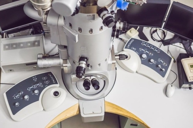
There are three principal types — SEM, TEM, and STEM — plus specialized variants built on each platform. All share the same core components: an electron source, electromagnetic lenses, a vacuum system, and a detector.
Scanning electron microscope (SEM)
A scanning electron microscope rasters a focused electron beam across the surface of the specimen in a rectangular grid, point by point. Each point in the grid emits secondary electrons (low-energy, from near the surface) and backscattered electrons (high-energy, carrying compositional information). A detector collects these in sync with the scan, building an image line by line.
The result is a beautifully three-dimensional surface image: the ant’s eye above is a classic SEM output. Surface texture, grain boundaries, fracture surfaces, and coating uniformity are all natural SEM territory. Specimens typically need to be electrically conductive — biological samples are coated with a few nanometers of gold or platinum — and must be dry, since the standard SEM operates under vacuum.
Cryo scanning electron microscope
Cryo-SEM extends the technique to hydrated, moisture-containing specimens — plants, food microstructure, biofilms, snowflakes. The specimen is plunge-frozen in liquid nitrogen so rapidly that water vitrifies (forms amorphous ice rather than damaging crystals), then transferred under cryogenic conditions to the SEM stage. The resulting images show the real hydrated architecture of the specimen, not the collapsed, dehydrated artifact that conventional fixation produces.
Electron backscatter diffraction
Used as an attachment on a standard SEM, an electron backscatter diffraction (EBSD) detector measures the diffraction pattern of electrons backscattered from the crystal lattice at each scan point. The result is a crystallographic map: orientation, grain boundaries, phase distribution, and texture across a polished cross-section — essential in metallurgy and geology for understanding how a material’s crystal structure governs its mechanical behavior.
Transmission electron microscope (TEM)
Where the SEM reads surface signals, the transmission electron microscope fires a broad electron beam straight through the specimen. The electrons that make it through — and the ways they are scattered, absorbed, or diffracted — carry the structural information that forms the image on a camera below.
For electrons to transmit through a solid, the specimen must be thin: generally below 100 nm, often in the 30–80 nm range. Reaching that thickness from a bulk sample requires considerable work — the ultramicrotome, focused ion beam milling, and electropolishing are all standard thinning routes. A tungsten field-emission gun provides the electron beam; it is accelerated by a high voltage (typically 80–300 kV), focused by a condenser lens system, passed through the specimen, and then re-focused by an objective lens onto a detector or phosphor screen. TEMs reveal internal structure: lattice planes, dislocations, precipitates, and grain boundaries invisible from the surface.
Electron tomography
By tilting a TEM specimen through a series of angles (typically ±70°) and recording a projection image at each tilt, then using back-projection algorithms to reconstruct the dataset, electron tomography builds a full 3D volume of the specimen at nanometer resolution. It is the electron-microscopy equivalent of a CT scan, and has been used to reconstruct entire neural synapses, nanoparticle shapes, and the internal pore structure of catalysts.
Reflection electron microscope
A reflection electron microscope (REM) uses a beam transmitted toward the surface at a glancing angle, forming an image from elastically backscattered electrons. The technique reveals surface reconstructions and step structures with exceptional sensitivity, and is often paired with reflection high-energy electron diffraction (RHEED) for real-time monitoring of thin-film growth during deposition.
Serial section electron microscopy
Serial section electron microscopy (sSEM) cuts a biological volume — a block of brain tissue, for instance — into hundreds or thousands of ultrathin sections and images each one. Stitched together computationally, the sections become a 3D map of neural connectivity. Large-scale connectomics projects have used sSEM to map the complete wiring of small sections of mammalian cortex at synaptic resolution.
Scanning transmission electron microscope (STEM)
The STEM combines the scanning approach of the SEM with the transmitting geometry of the TEM. A finely focused electron probe scans across a thin specimen point by point, and detectors at different angles collect the transmitted electrons simultaneously.
The most important STEM mode for atom imaging is High-Angle Annular Dark-Field (HAADF). In HAADF-STEM, a ring-shaped detector collects electrons scattered to high angles. The intensity at each pixel scales approximately with the square of the atomic number (Z²) of the atoms in that column — a phenomenon called Z-contrast. On the resulting image, heavy atoms appear bright; light atoms appear dark or nearly invisible. A single heavy-metal atom substituted into a crystal lattice appears as a bright dot against a darker background, its position pinpointing its exact location in the atomic structure. This is the specific technique behind virtually every famous “see single atoms” image you have encountered online.
STEMs are also uniquely compatible with spectroscopy: EDS and EELS detectors can identify the chemical element at every scan pixel, producing atomically resolved composition maps — a periodic table overlaid on an atomic-resolution image.
The development of electron microscopes
The story of atom microscopy — a chapter in the broader history and growth of microscopy — runs through a handful of decisive experiments and three Nobel Prizes, each one expanding the boundary of what human beings can observe.
The first electron microscope

In 1931, physicist Ernst Ruska and electrical engineer Max Knoll built the first working electron microscope in Berlin. The 1931 prototype was a proof of principle capable of a few hundred times magnification — impressive for a first attempt, but not yet competitive with glass lenses. By 1933, Ruska had developed a refined instrument that surpassed the resolution of any light microscope for the first time in history (Britannica). That milestone earned Ruska the 1986 Nobel Prize in Physics, half shared with Gerd Binnig and Heinrich Rohrer, who had separately invented the scanning tunneling microscope (Nobel Prize in Physics 1986).
Several other figures contributed to the electron microscope’s foundation: Hans Busch developed the electromagnetic lens in 1926–1927; Leó Szilárd and Dennis Gabor applied for an EM patent; and Reinhold Rudenberg obtained a patent in 1931 for a practical electron microscope design.
Developments on the first design
The scanning electron microscope principle was demonstrated by Manfred von Ardenne in 1937. Siemens produced the first commercial TEM in 1939; researchers at the University of Toronto (Burton, Hall, Hillier, and Prebus) had built an independently developed practical instrument in 1938. In the decades that followed, improvements in electron guns, lens design, and vibration isolation pushed resolution incrementally lower, until aberration correction in the 2000s broke the 1-Ångström barrier and opened the sub-atomic-column imaging era.
Landmark milestones in atom-scale imaging
Three moments mark the progression from seeing atoms to manipulating them:
- 1989 — IBM spells its name in atoms. Don Eigler and Erhard Schweizer at IBM Almaden used a scanning tunneling microscope at 4 kelvin to position 35 individual xenon atoms on a nickel surface, spelling “IBM” — the first deliberate, controlled manipulation of single atoms (Phys.org). The atoms were moved by lowering the STM tip close enough to interact with a xenon atom’s van der Waals forces, then sliding it laterally across the surface.
- 2010 — first direct imaging of single light atoms. Ondrej Krivanek and colleagues imaged single atoms of boron and nitrogen in graphene using an aberration-corrected STEM — the first time individual atoms lighter than silicon had been directly imaged.
- 2018 — 0.39 Å world resolution record. Cornell’s Muller group used a 4D-STEM detector (the EMPAD) with electron ptychography reconstruction to achieve 0.39 Å resolution — finer than the diameter of a hydrogen atom. In 2021 they pushed further with 3D imaging of a praseodymium orthoscandate crystal at similar precision.
Other microscopes that can see atoms and beyond
Electron microscopes image atoms through the specimen. Scanning probe microscopes feel the surface at atomic resolution — and can move atoms as the IBM experiment demonstrated.
Scanning probe microscope
A scanning probe microscope works by bringing a nanoscale tip to within a fraction of a nanometer of the specimen surface and measuring an interaction signal as the tip scans across. There is no lens, no electron beam — just a mechanical finger reading the atomic landscape. There are three principal types:
- Atomic force microscope (AFM) — a cantilever with a tip a few atoms wide is deflected by atomic-scale forces (van der Waals, electrostatic, chemical bonding) as it tracks the surface. The deflection is measured by reflecting a laser off the cantilever back. AFM produces true 3D topographic maps of surfaces at atomic resolution and — unlike SEM or TEM — works in air and in liquid, making it the go-to tool for imaging biological membranes and DNA.
- Scanning tunneling microscope (STM) — a sharp metal tip is brought within roughly 1 nm of a conducting surface. At that distance, electrons quantum-mechanically tunnel across the gap, producing a measurable tunneling current that drops exponentially with distance. Sub-ångström changes in gap width produce measurable current changes, giving the STM extraordinary vertical sensitivity. STMs can image atomic orbitals directly and, as IBM demonstrated, move individual atoms. They require a conductive specimen and typically ultra-high vacuum.
- Magnetic force microscope (MFM) — the tip is magnetized; as it scans slightly above the surface, magnetic dipole forces between tip and specimen deflect the cantilever, mapping the magnetic domain structure of the surface. Used heavily in data-storage research to image the bits on hard disk platters.
What an atom actually looks like under a microscope
This is the question the original version of this page promised to answer and then didn’t. Here is an honest description.
In a HAADF-STEM image of a crystalline material, individual heavy atoms appear as bright white or yellow dots against a dark or near-black background, arranged in the regular grid of the crystal lattice. The brightness scales with atomic weight: a gold atom is noticeably brighter than a neighboring silver atom; a carbon atom may be barely visible next to a cobalt atom. The dots are not fuzzy blobs — in a well-aligned, aberration-corrected instrument, each atomic column is resolved as a distinct peak, and the spacing between adjacent columns (typically 1.5–3 Å in common materials) is clearly measurable.
What you are usually looking at is an atomic column — dozens to hundreds of atoms stacked directly behind each other along the direction the electron beam travels. The “dot” is their combined projected signal. In special circumstances — a single metal atom adsorbed on a surface, or a dopant substituted into a 2D material like graphene — you are looking at a genuinely isolated atom.
In cryo-EM images of proteins, atoms appear as density blobs in an electron-density map reconstructed from thousands of particle images. Individual atoms are typically not resolved as separate peaks in cryo-EM (resolution is usually 2–4 Å, not sub-Ångström), but the positions of secondary-structure elements — alpha helices, beta sheets — are directly visible and the side chains of amino acids become interpretable at high resolution.
What are the disadvantages of electron microscopes?
Electron microscopes have transformed science. They also come with significant practical limitations that shape how and where they are used.
Cost of production
A research-grade aberration-corrected STEM or TEM costs $3–$10 million and requires a dedicated facility — not necessarily underground, but certainly in a vibration-isolated room with tight control of electromagnetic interference, temperature, and acoustic noise. Even a mid-range analytical TEM runs $500k–$2M. The instruments are rare not because they are mythically few in number — there are thousands of electron microscopes at universities, national laboratories, and semiconductor facilities worldwide — but because sub-ångström instruments capable of true atomic imaging are expensive enough that most institutions share access through core facilities (see our guide to electron microscope cost).
Viewing environment
Standard TEMs and SEMs require high vacuum inside the column. Air molecules would scatter the electron beam and make imaging impossible. That means gaseous and liquid specimens cannot be imaged directly in a conventional instrument. Environmental SEMs (ESEM) and liquid-phase TEM holders have addressed this partially, but they represent specialized configurations with resolution trade-offs.
Specimen preparation
Sample preparation for TEM is the discipline’s hardest craft. To reach electron-transparency (below ~100 nm thick), a bulk metal, ceramic, or biological block must be thinned by ion beam milling, electropolishing, or ultramicrotomy. Each technique introduces its own artifacts: ion milling can implant gallium ions from the FIB beam; chemical fixation used in biological prep can cross-link proteins in unnatural conformations. Common preparation steps and what they actually do:
- Ultrathin sectioning — a diamond knife on an ultramicrotome cuts slices as thin as 30 nm for biological blocks embedded in resin.
- Conductive coating — 2–5 nm of gold, platinum, or carbon prevents charge build-up on insulating SEM specimens that would otherwise deflect the beam.
- Cryofixation / vitrification — plunge-freezing biological samples in liquid ethane cools so rapidly (~10,000 °C/s) that water vitrifies instead of crystallizing, locking cells and proteins in near-native state.
- Chemical fixation — glutaraldehyde and osmium tetroxide cross-link proteins and lipids to preserve structure during subsequent dehydration steps; introduces known chemical artifacts.
- Staining — heavy-metal stains (uranyl acetate, lead citrate) bind to specific cellular structures, increasing their electron contrast.
- FIB milling — a focused ion beam (gallium ions) mills a thin lamella directly from a bulk specimen, enabling site-specific TEM preparation from any surface location, including a specific transistor on a semiconductor chip.
Can a regular person access an electron microscope?
More easily than most people assume. Options include:
- University core facilities — most research universities with materials science or biology programs operate shared electron microscopy facilities that offer fee-for-service imaging. Rates vary but a few hundred dollars per day of SEM time is common.
- National laboratory user programs — facilities like Argonne’s Center for Nanoscale Materials or NIST’s Center for Nanoscale Science and Technology offer competitive access to world-class instruments for qualifying research projects.
- Desktop / benchtop SEMs — instruments from Hitachi (TM3030/TM4000 series) and Coxem (EM-30) start around $30,000–$60,000 and achieve 17–30 nm resolution — far short of atomic resolution, but sufficient for surface morphology, particle sizing, and quality control. Some high schools and community colleges now own one.
Frequently asked questions
Can you see an atom with an electron microscope?
Yes — in a HAADF-STEM, individual heavy atoms and atomic columns appear as bright dots against a dark background. The images are signal reconstructions, not conventional photographs, and a “dot” often represents a column of atoms stacked along the beam direction rather than a single isolated atom.
What does an atom look like under a microscope?
In HAADF-STEM images, atoms appear as bright spots arranged in the regular pattern of the crystal lattice. Heavier atoms are brighter. Spacing between adjacent spots is typically 1–3 ångströms. In cryo-EM images of proteins, atoms appear as overlapping density blobs rather than discrete peaks.
What is the most powerful microscope for seeing atoms?
Aberration-corrected STEM instruments hold the resolution record at 0.39 Å (Cornell, 2018). For manipulating rather than imaging, the scanning tunneling microscope is the tool of choice — it was used to position individual xenon atoms in the 1989 IBM experiment.
How does a scanning tunneling microscope see atoms?
It does not use light or electrons as a beam. Instead, a sharp metal tip is brought to within ~1 nm of a conducting surface, and a quantum-mechanical tunneling current flows across the gap. That current is exponentially sensitive to the tip-surface distance, so sub-ångström height changes produce measurable current changes. The result is an atomic-resolution topographic map of the surface.
Can a light microscope see atoms? Why not?
No. The Abbe diffraction limit for visible light is approximately 200 nm. Atoms measure 0.1–0.3 nm across — roughly 1000 times smaller than what visible light can resolve. No amount of engineering can get a light microscope below this physical limit.
What is the resolution of an electron microscope?
It depends heavily on type and configuration. A standard SEM resolves ~1–20 nm. A conventional TEM resolves ~0.1–0.2 nm. An aberration-corrected STEM can reach 0.05 nm (0.5 Å) routinely, and 0.039 nm (0.39 Å) at the current world record.
Who invented the electron microscope?
Ernst Ruska and Max Knoll built the first working electron microscope in 1931. Ruska received the 1986 Nobel Prize in Physics for this work, sharing it with Gerd Binnig and Heinrich Rohrer who invented the scanning tunneling microscope.
How much does an electron microscope cost?
Benchtop SEMs start around $30,000–$60,000. Full analytical SEMs run $100k–$500k. Research TEMs and STEMs cost $500k–$10M+, with aberration-corrected instruments at the high end. Most researchers access high-end instruments through shared university or national-laboratory facilities.
Conclusion
Atom microscopy began as a physicist’s experiment in 1931 and grew into the technical foundation of modern materials science, semiconductor manufacturing, structural biology, and nanotechnology. Electron microscopes — SEM, TEM, and STEM — resolve features from the micrometer scale down to fractions of an ångström, using beams of electrons whose short de Broglie wavelength defeats the diffraction barrier that stops light microscopy at 200 nm. Scanning probe microscopes extend the reach further, feeling and moving individual atoms on surfaces. Three Nobel Prizes (1986, 2017, and the 2017 Chemistry Prize for cryo-EM) mark the field’s impact on science as a whole.
The images that result — bright atomic columns arranged in crystal lattices, protein structures emerging from cryo-EM reconstructions, IBM’s xenon-atom logo — are not science fiction. They are engineering made possible by controlling electrons at the scale of picometers, inside instruments that must be quieter and more stable than almost anything else humanity builds.
Originally posted 2026-04-07 01:59:48.